WELCOME TO NANOFAB.SDSU
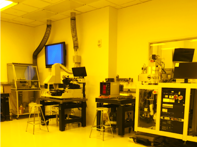
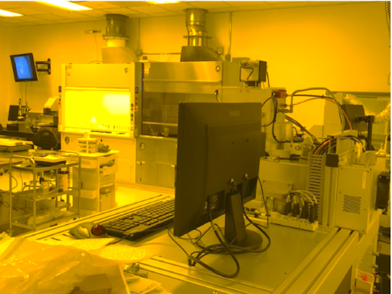
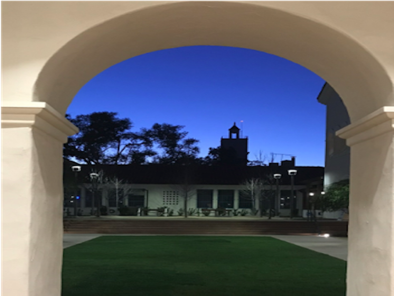
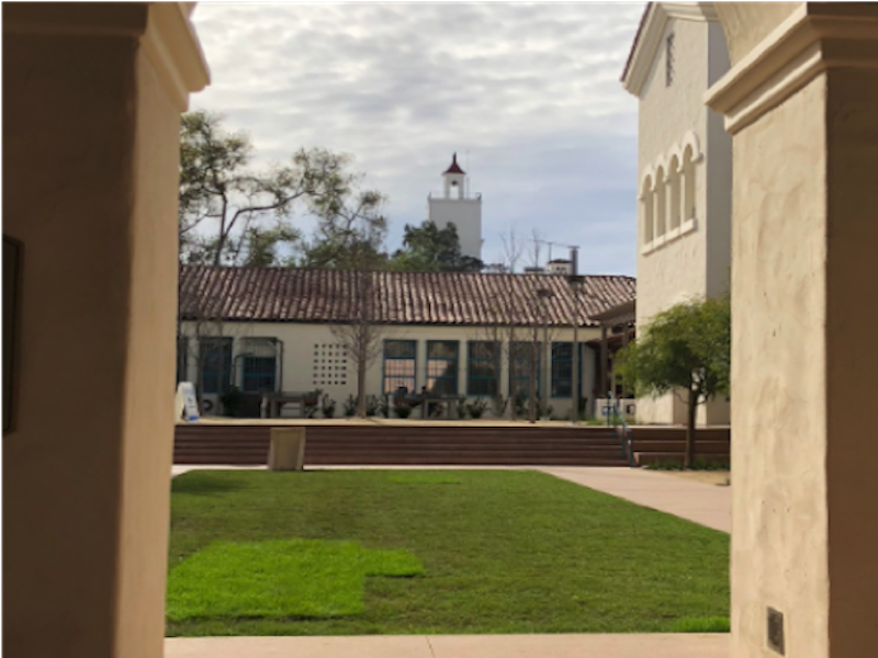
Welcome to NanoFab.SDSU, a brand-new leading center for micro and nanofabrication located in the EIS building of SDSU. The state-of-the-art facility has a 2500 sq. ft. ISO 9001-certified Class 1000 Cleanroom with 4” and 6” wafer processing capability with 0.2 micron lithography feature sizes. The Center provides a comprehensive and expanding selection of state-of-the-art process equipment for lithography, etching, thermal processing, thin-film deposition, and characterization. The vision of the Center is to become a leading national and international center of integrated silicon and polymer/carbon-based micro and nanofabrication facility to support user needs in newer areas of nanoscale science, engineering, and technology domains. The Center has a strong focus on educating undergraduate, masters and doctoral students in the various areas of nanotechnology.
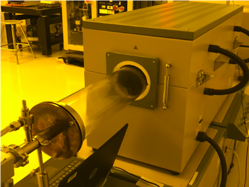
Equipment & Facilities
- ABM, High Resolution Mask Alignment and Exposure System (0.2 micron resolution)
- PECVD & Pyrolysis Split-Tube Furnace with Vacuum
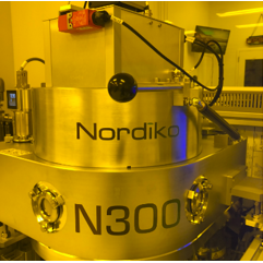
- Nordiko Metal Deposition System. Co-deposition of up to 4 metals.
- Technics Series 85 DRIE and Plasma Etcher
- OAI UV Light Source
- Brewer Spin-coater
- ETS-150 Thermal Evaporation + Sputtering
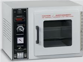
- High-temperature ovens
- Signatone Probe Station and 4-Point Probe
- Filmetrics F40-PAR Profilometer
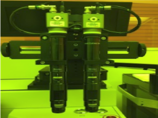
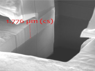
- Hirox 3D Microscope
- Newport Solar Simulator with Oriel I-V Station
Management
Director of Center
Professor Sam Kassegne
kassegne@sdsu.edu
Capabilities
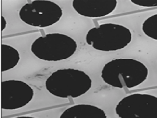
- CVD/PECVD for Dielectric Materials
- DRIE
- Wet and Dry Oxide Growth
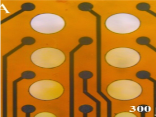
- Thin-film Metal Deposition (Au, Pt, Cr, Ti, Ni, Cu)
- Graphene, Glassy Carbon, CNT
- Acid (Wet) Etching
- Pyrolysis
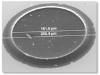
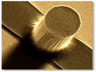
- SEM and 3D Microscopy
SERVICES
Major Achievements
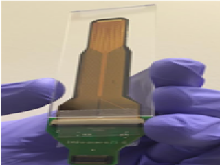
- Several patents and disclosures in MEMS IMU, organic solar cells, neural probes, and graphene processes.
- Incubated start-ups and licensed variety of technology
- Unique strength in integrating carbon, polymer, and silicon-based microfabrication.
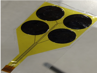
- First to introduce single and double-sided pattern transfer technology for carbon microelectrodes on polymer substrates
- Hosted CMEMS 2018 Conference.
- Training next generation of workforce and researchers (alumni work in Apple, Intel, Qualcomm, ASML and several start-ups).
- Funded by NSF, DoE, DoD and Industry
Offering Services To:
Industry
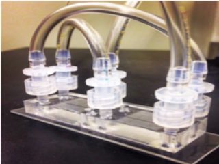
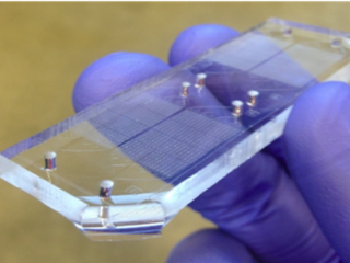
- TumorGen MDx (microfluidics chips)
- TissueNetix (microfluidics chips)
- Grapheton
Research Labs
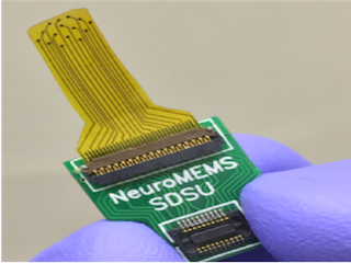
- University of Washington (CSNE) – (cortical and spinal neural probes)
- University of Texas at Dallas
- Physikalisch-Technische Bundesanstalt (PTB) Braunschweig, Berlin, Germany
- University of Ferrara – (ECoG Neural Probes, 12, 32, and 64-channels)
- University of Indonesia
- Yonezawa University (Japan)
- SPAWAR, SSC-Pacific, US Navy
MEMBERSHIP
Advantages of Membership
- Direct access to highly-trained students
- Interaction with leading researchers
- State-of-the-art equipment and processes
- Participate in annual Industry Day�
- Reduced rate for members
- Simple paperwork
- No institutional barriers
- Your IP is protected
- Opportunity to license IP from consortium labs.
PORTFOLIO
CONTACT
- Sam Kassegne, PhD, PE
Professor of Mechanical Engineering,
Deputy Director, NSF Center for Sensorimotor Neural Engineering
Department of Mechanical Engineering
San Diego State University
5500 Campanile Drive, EIS - 214
San Diego, CA 92182, USA
kassegne at sdsu dot edu